Search photos...
Custom work
All
Photos
Illustrations
Designs
Collections
Contributors
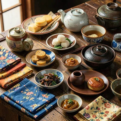
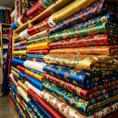
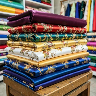
fabric layers
Orientation
Color
Exclude
Features
Sort by
textile
colors
traditional
panamanian
mola
illustration
+4 more
panama
kuna
guna
reverse
Rosa Pigmento
Download
Rosa Pigmento
Download
Ayesha Malik
Download
Fatima Rahman
Download
Fatima Rahman
Download
Nan O'Gate
Download
Nan O'Gate
Download
Nan O'Gate
Download
Priya Mehra
Download
Reg Overprint
Download
Chidi Okonkwo
Download
Sable Wynn
Download
Mesh Tensegrity
Download
Awa Diallo
Download
Haruki Noda
Download
Nan O'Gate
Download
Nan O'Gate
Download
Nan O'Gate
Download
Nan O'Gate
Download
Nan O'Gate
Download
Nan O'Gate
Download
Nan O'Gate
Download
Nan O'Gate
Download
Nan O'Gate
Download
Nan O'Gate
Download
Nan O'Gate
Download
Nan O'Gate
Download
Nan O'Gate
Download
Nan O'Gate
Download
Nan O'Gate
Download
Nan O'Gate
Download
Nan O'Gate
Download
Nan O'Gate
Download
Nan O'Gate
Download
Nan O'Gate
Download
Nan O'Gate
Download
Nan O'Gate
Download
Nan O'Gate
Download
Nan O'Gate
Download
Nan O'Gate
Download
Nan O'Gate
Download
Nan O'Gate
Download
Nan O'Gate
Download
Nan O'Gate
Download
Nan O'Gate
Download
Nan O'Gate
Download
Nan O'Gate
Download
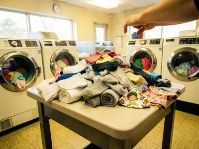
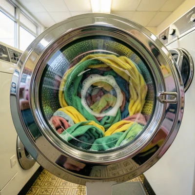
Spin Cycle
Download
Spin Cycle
Download
Haruki Noda
Download
Rosa Pigmento
Rosa Pigmento
Ayesha Malik
Fatima Rahman
Fatima Rahman
Nan O'Gate
Nan O'Gate
Nan O'Gate
Priya Mehra
Reg Overprint
Chidi Okonkwo
Sable Wynn
Mesh Tensegrity
Awa Diallo
Haruki Noda
Nan O'Gate
Nan O'Gate
Nan O'Gate
Nan O'Gate
Nan O'Gate
Nan O'Gate
Nan O'Gate
Nan O'Gate
Nan O'Gate
Nan O'Gate
Nan O'Gate
Nan O'Gate
Nan O'Gate
Nan O'Gate
Nan O'Gate
Nan O'Gate
Nan O'Gate
Nan O'Gate
Nan O'Gate
Nan O'Gate
Nan O'Gate
Nan O'Gate
Nan O'Gate
Nan O'Gate
Nan O'Gate
Nan O'Gate
Nan O'Gate
Nan O'Gate
Nan O'Gate
Nan O'Gate
Nan O'Gate
Nan O'Gate
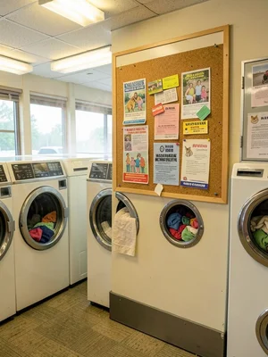
Spin Cycle
Spin Cycle
Haruki Noda
Refine with AI