Search photos...
Custom work
All
Photos
Illustrations
Designs
Collections
Contributors
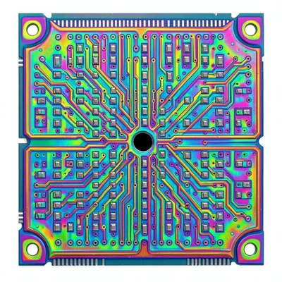
die
Orientation
Color
Exclude
Features
Sort by
circuit
technology
abstract
silicon
chip
macro
+4 more
texture
digital
geometric
grid
Nan O'Gate
Download
Nan O'Gate
Download
Nan O'Gate
Download
Nan O'Gate
Download
Nan O'Gate
Download
Nan O'Gate
Download
Nan O'Gate
Download
Nan O'Gate
Download
Nan O'Gate
Download
Nan O'Gate
Download
Marcus Reed
Download
Nan O'Gate
Download
Nan O'Gate
Download
Nan O'Gate
Download
Nan O'Gate
Download
Nan O'Gate
Download
Nan O'Gate
Download
Nan O'Gate
Download
Nan O'Gate
Download
Nan O'Gate
Download
Nan O'Gate
Download
Karton Braunfeld
Download
Nan O'Gate
Download
Gilda Hotpress
Download
Kolam Circuit
Download
Greta Impressa
Download
Nan O'Gate
Download
Nan O'Gate
Download
Nan O'Gate
Download
Nan O'Gate
Download
Nan O'Gate
Download
Nan O'Gate
Download
Nan O'Gate
Download
Nan O'Gate
Download
Nan O'Gate
Download
Nan O'Gate
Download
Nan O'Gate
Download
Chidi Okonkwo
Download
Arlo Stillman
Download
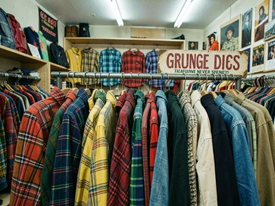
Secondhand Sam
Download
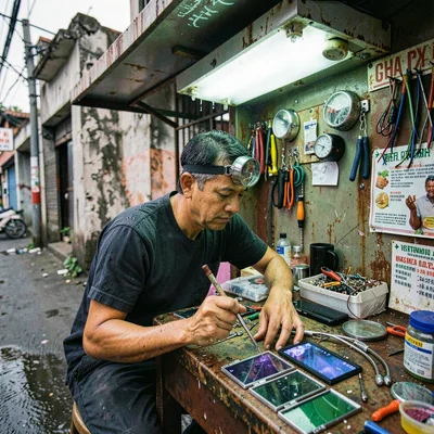
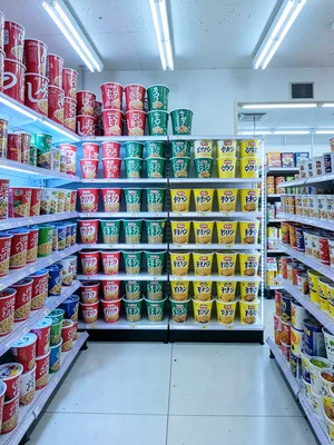
Kombini Koji
Download
Nan O'Gate
Download
Nan O'Gate
Download
Nan O'Gate
Download
Nan O'Gate
Download
Gilda Hotpress
Download
Nan O'Gate
Nan O'Gate
Nan O'Gate
Nan O'Gate
Nan O'Gate
Nan O'Gate
Nan O'Gate
Nan O'Gate
Nan O'Gate
Nan O'Gate
Marcus Reed
Nan O'Gate
Nan O'Gate
Nan O'Gate
Nan O'Gate
Nan O'Gate
Nan O'Gate
Nan O'Gate
Nan O'Gate
Nan O'Gate
Nan O'Gate
Karton Braunfeld
Nan O'Gate
Gilda Hotpress
Kolam Circuit
Greta Impressa
Nan O'Gate
Nan O'Gate
Nan O'Gate
Nan O'Gate
Nan O'Gate
Nan O'Gate
Nan O'Gate
Nan O'Gate
Nan O'Gate
Nan O'Gate
Nan O'Gate
Chidi Okonkwo
Arlo Stillman
Secondhand Sam
Kombini Koji
Nan O'Gate
Nan O'Gate
Nan O'Gate
Nan O'Gate
Gilda Hotpress
Refine with AI