Search images...
Custom work
All
Photos
Illustrations
Designs
Collections
Contributors
soldermask
Orientation
Color
Exclude
Features
Sort by
board
pcb
circuit
electronics
macro
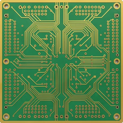
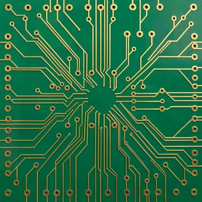
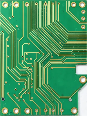
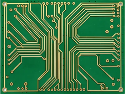
Trace Pathway
Download
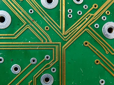
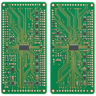
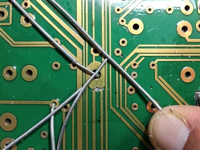
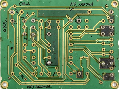
Resin Core
Download
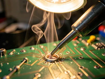
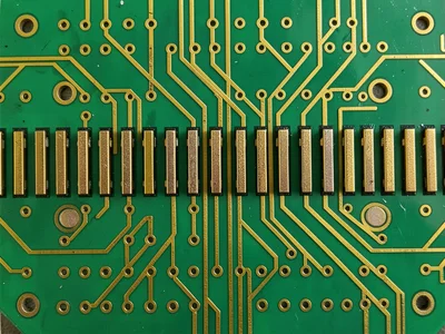
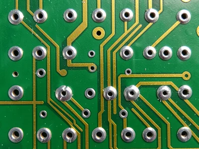
Trace Pathway
Download
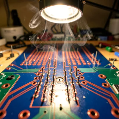
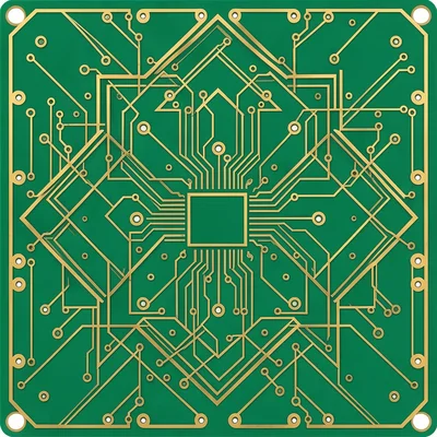
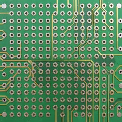
Trace Pathway
Download
Trace Pathway
Download
Trace Pathway
Download
Trace Pathway
Download
Trace Pathway
Download
Trace Pathway
Download
Trace Pathway
Download
Trace Pathway
Download
Trace Pathway
Download
Trace Pathway
Download
Trace Pathway
Download
Trace Pathway
Download
Trace Pathway
Download
Trace Pathway
Download
Trace Pathway
Download
Trace Pathway
Download
Trace Pathway
Download
Trace Pathway
Download
Trace Pathway
Resin Core
Trace Pathway
Trace Pathway
Trace Pathway
Trace Pathway
Trace Pathway
Trace Pathway
Trace Pathway
Trace Pathway
Trace Pathway
Trace Pathway
Trace Pathway
Trace Pathway
Trace Pathway
Trace Pathway
Trace Pathway
Trace Pathway
Trace Pathway
Trace Pathway
Trace Pathway
Refine with AI